Elevating Our Electronics: Why We Choose Cutting‑Edge Circuit Boards for Success
We are also pleased to tell you how we have incorporated the advanced PCB solutions into our pursuit to provide consistent, high-quality electronics. In this blog, we explore our experiences with double‑sided printed circuit boards, high‑speed designs, and high‑density HDI circuit board manufacturers. We tell how we believe in the BS Interconn in providing quality circuit technology, and how our decisions drive our product excellence.
Our PCB Journey: Better Performance Starts Here
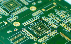
Printed circuit boards form the very backbone of our device designs. In particular, double‑sided printed circuit boards serve our needs brilliantly. These boards have two conductive layers, top and bottom, and a solder mask insulation to protect and interconnect our circuits in a clean manner. They have flexible layouts and can handle current ranging between milliamps and several amps with a thickness of between 0.031 and 0.125 inches. For our UI and control boards, they offer whatever versatility, density, and performance we need.
The major difference between a double-sided PCB and a single-sided board is clear to us in our work. Single-layer PCBs can only use one side of the copper traces and components. In contrast, on the double-sided designs, we have copper and components on both sides, so we can route traces over each other, even without solder bridges, or with no point-to-point wiring. We would like this more, though it is more complex, because it is dense and reliable. Added complexity is worth it in the form of small, durable devices.
High‑Speed Circuit Boards: When Timing Matters Most
Printed circuit boards form the very backbone of our device designs. In particular, double‑sided printed circuit boards serve our needs brilliantly. These boards have two conductive layers, top and bottom and a solder mask insulation to protect and interconnect our circuits in a clean manner. They have flexible layouts and can handle current ranging between milliamps and several amps with a thickness of between 0.031 and 0.125 inches. For our UI and control boards, they offer whatever versatility, density, and performance we need.
The major difference between a double-sided PCB and a single-sided board is clear to us in our work. Single-layer PCBs can only use one side of the copper traces and components. In contrast, on the double-sided designs, we have copper and components on both sides, so we can route traces over each other, even without solder bridges, or with no point-to-point wiring. We would like this more, though it is more complex, because it is dense and reliable. Added complexity is worth it in the form of small, durable devices.
High‑Density Circuit PCB Design: Small Footprint, Big Capability
When designing small electronics, we resort to the high-density circuit PCB techniques, or to the HDI (high-density interconnect). These boards allow us to get more connection points into a smaller space, layering components, and shrinking interconnect spaces geometrically. We have new designs that have target pads as thin as 175m with 75m diameter laser holes. Consistency between image transfer, pressing, and laser drilling to within a total offset of less than 40 0m is needed to prevent alignment errors or CAF defects.
We have collaborated with the industry leaders in the high-density circuit PCBs, which can provide laser-drilled blind vias. Where our projects require greater voltage tolerance, or thicker dielectric layers, or larger current-carrying vias, we employ mechanical blind-via techniques instead–drill through-holes, plug them with resin, then laminate inner layers and finish like a multilayer board. Using these methods, we can achieve density and reliability benchmarks that traditional PCB approaches cannot.
Why We Trust BS Interconn for Circuit Board Solutions
Because their PCB manufacturing offers the specifications and service that match our growing needs:
- Double‑sided circuit boards: 2‑layer normal FR‑4, 0.6 mm dielectric, 1 oz copper, min track & gap 0.15 mm—ideal for user interface and control boards.
- 6‑layer high‑speed boards: Using EM‑528BK low-loss material, controlled impedance, ENIG finish, 2 oz copper, 0.12 mm track/gap—perfect for telecom and signal‑sensitive designs.
- 10‑layer high‑density boards: Laser drilling, mechanical blind vias, 0.075 mm track/gap, 1.5 oz copper, ENIG finish—designed for ultra‑compact interconnects.
As one of the reputable HDI Circuit Board Manufacturers, it consistently supplies precision boards meeting our technical standards. We value their ability to deliver high-quality, low-loss, and high-density circuit boards—whenever we need them. We rarely mention the brand, but we do acknowledge their strong support and flexibility in tailored solutions. We use their services for critical layers up to ten, trusting their accuracy, quality control, and delivery.
Frequently Asked Questions
Q: Why is a double-sided PCB superior to a single-sided PCB?
A: We have greater routing flexibility, greater component density, and fewer wiring woes. Although the complexity of the fabrication is high, the possibility is more than the single-sided constraints.
Q: Do we do small vias and small tolerances?
A: Yes. We have laser-drilled blind vias on our high-density circuit PCB solutions to 75um, and the strict alignment between processes of less than 40um, with no short-circuits or defects.
Q: What is the reason for the utilization of EM‑528BK material in high-speed boards?
A: EM -528BK reduces insertion loss by approximately 15 percent at 20 GHz compared to FR -4. With controlled impedance of 0.5% to 5% it guarantees signal integrity on telecom and data-sensitive applications.
Ready to Elevate Your Electronics with Top‑Tier PCBs?
We have faith in creating brilliant electronics that work exceptionally well, on signal integrity, space, and reliability. By using the right printed circuit boards—double‑sided, high‑speed, or high‑density—and working with qualified BS Interconn HDI circuit board manufacturers, we ensure our designs meet and exceed expectations.
We want to develop your next PCB project with you using quality PCB solutions. Reach out to us today!
Also Read Us- theglobalnewz.com